(Hong Kong)

Product Summary
Features and Benefits
High Capacity
? 15 k to 1 M System Gates
? Up to 144 kbits of True Dual-Port SRAM
? Up to 300 User I/Os
Reprogrammable Flash Technology
? 130-nm, 7-Layer Metal (6 Copper), Flash-Based CMOS
Process
? Instant On Level 0 Support
? Single-Chip Solution
? Retains Programmed Design when Powered Off
High Performance
? 350 MHz System Performance
? 3.3 V, 66 MHz 64-Bit PCI?
In-System Programming (ISP) and Security
? ISP Using On-Chip 128-Bit Advanced Encryption Standard
(AES) Decryption (except ARM?-enabled ProASIC?3 devices)
via JTAG (IEEE 1532–compliant)?
? FlashLock? to Secure FPGA Contents
Low Power
? Core Voltage for Low Power
? Support for 1.5 V-Only Systems
? Low-Impedance Flash Switches
High-Performance Routing Hierarchy
? Segmented, Hierarchical Routing and Clock Structure
Parametrics
Jeff Jia
Sales Manager
GUI GUANG INTERNATIONAL TRADE LIMITED
www.ggichk.com
E-mail:jeff@ggichk.com
Tel:0086-15816677110
Fax:00852-35902333
Features
Advanced I/O
? 700 Mbps DDR, LVDS-Capable I/Os (A3P250 and above)
? 1.5 V, 1.8 V, 2.5 V, and 3.3 V Mixed-Voltage Operation
? Wide Range Power Supply Voltage Support per JESD8-B,
Allowing I/Os to Operate from 2.7 V to 3.6 V
? Bank-Selectable I/O Voltages—up to 4 Banks per Chip
? Single-Ended I/O Standards: LVTTL, LVCMOS 3.3 V /
2.5 V / 1.8 V / 1.5 V, 3.3 V PCI / 3.3 V PCI-X?
and LVCMOS
2.5 V / 5.0 V Input
? Differential I/O Standards: LVPECL, LVDS, B-LVDS, and
M-LVDS (A3P250 and above)
? I/O Registers on Input, Output, and Enable Paths
? Hot-Swappable and Cold Sparing I/Os?
? Programmable Output Slew Rate?
and Drive Strength
? Weak Pull-Up/-Down
? IEEE 1149.1 (JTAG) Boundary Scan Test
? Pin-Compatible Packages across the ProASIC3 Family
Clock Conditioning Circuit (CCC) and PLL?
? Six CCC Blocks, One with an Integrated PLL
? Configurable Phase-Shift, Multiply/Divide, Delay Capabilities
and External Feedback
? Wide Input Frequency Range (1.5 MHz to 350 MHz)
Embedded Memory?
? 1 kbit of FlashROM User Nonvolatile Memory
? SRAMs and FIFOs with Variable-Aspect-Ratio 4,608-Bit RAM
Blocks (×1, ×2, ×4, ×9, and ×18 organizations)?
? True Dual-Port SRAM (except ×18)
ARM Processor Support in ProASIC3 FPGAs
? M1 ProASIC3 Devices—ARM?Cortex?-M1 Soft Processor
Available with or without Debug
Diagrams
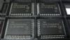
| Image | Part No | Mfg | Description |  |
Pricing (USD) |
Quantity | ||||||
|---|---|---|---|---|---|---|---|---|---|---|---|---|
 |
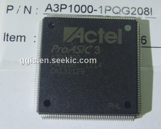
 A3P1000-1PQG208I |
|
IC FPGA 1KB FLASH 1M 208-PQFP |
Data Sheet |
|
|
||||||
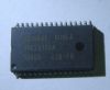
| Image | Part No | Mfg | Description | |
Pricing (USD) |
Quantity | ||||||
|
A3P1000 |
Other |
|
Data Sheet |
Negotiable |
|
||||||
|
A3P1000-1FG144 |
|
IC FPGA 1KB FLASH 1M 144-FBGA |
Data Sheet |
|
|
||||||
|
A3P1000-1FG144I |
|
IC FPGA 1KB FLASH 1M 144-FBGA |
Data Sheet |
|
|
||||||
|
A3P1000-1FG144T |
|
IC FPGA 1KB FLASH 1M 144-FBGA |
Data Sheet |
|
|
||||||
|
A3P1000-1FG256 |
|
IC FPGA 1KB FLASH 1M 256-FBGA |
Data Sheet |
|
|
||||||
|
A3P1000-1FG256I |
|
IC FPGA 1KB FLASH 1M 256-FBGA |
Data Sheet |
|
|
||||||